NCP1603
http://onsemi.com
17
The recommended biasing schematic of the controller is in
Figure 47 while a typical completed application schematic
can be referred to Figure 45. These two dies have their own
individual supply voltages at Pin 8 and Pin 14. The grounds
of the two dies are physically connected through the package
substrate but they are needed to be connected externally. The
bias voltage to the NCP1603 comes from the bulk voltage
V
bulk
through the HV pin (Pin 16) during startup. After
startup, a secondstage flyback transformer auxiliary winding
delivers the supply voltage to V
CC
.
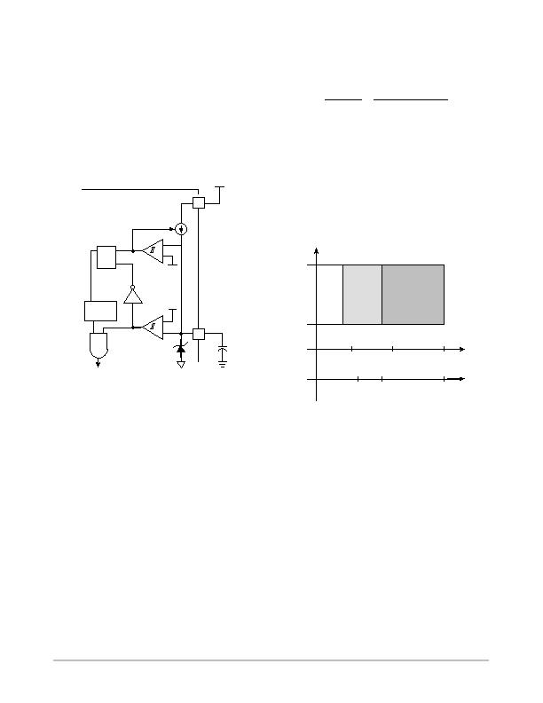
Lossless High Voltage Startup Circuit
Figure 48. V
CC2
Management
Q S
R
Double
Hiccup
B2
Counter
&
Turn Off
+
-
UVLO
3.2 mA
16
V
bulk
HV
12.6/
5.6 V
+
-
7.7 V
20 V
14
V
CC
Turn on Internal Bias
The HV pin (Pin 16) is capable of the maximum 500 V so
that this pin can be directly connected to the bulk voltage
V
bulk
and delivers startup supply voltage to the controller.
Figure 48 illustrates the block diagram of the startup circuit.
An UVLO comparator monitors the V
CC
at Pin 14. A startup
current source is activated and deactivated whenever the
voltage reaches V
CC2(latch)
(5.6 V typical) and V
CC2(on)
(12.6 V typical) thresholds respectively. Therefore, the V
CC
never drops below V
CC2(latch)
after powering up unless the
circuit is unplugged (i.e., V
bulk
disappears or smaller than its
minimum required operating threshold V
start(min)
(20 V
typical)). This feature makes the controller memorize the
external latch off function implemented in Pin 3.
This inchip startup circuit can minimize the number of
external components and Printed Circuit Board (PCB) area.
It also minimizes the loss due to startup resistor because
startup resistor always dissipates power but this startup circuit
can be turned off when the V
CC
voltage is sufficient. Actually,
there is a small leakage current I
HV3
(30 mA typical at
HV = 700 V) when the startup circuit is off.
The V
CC
capacitor is recommended to be at least 47 mF to
ensure that V
CC
is always above the minimum operating
voltage V
CC2(off)
(7.7 V typical) in the startup phase. For
example, the PWM die consumes I
CC2(op2)
(2.2 mA typical),
a 47 mF V
CC
capacitor can maintain the V
CC
above 7.7 V for
105 ms. It is the available time to establish a V
CC
voltage
from the flyback transformer auxiliary winding.
t
startup
+
C
VCC
DV
I
CC2(op2)
+
47 mF?12.6 V7.7 V)
2.2 mA
+ 105 ms
(eq. 1)
A large enough V
CC
capacitor can also help to maintain
V
CC2
always above V
CC2(off)
to prevent the IC accidentally
powered off during the standby condition where the
lowfrequency ripple of V
CC2
can be very high.
The PFC section does not consume any current in the
startup phase since V
aux
is disabled initially (i.e., V
aux
=
V
CC1
= 0 V).
When V
CC2
falls below V
CC2(off)
(7.7 V typical) for
whatever reason, the PWM section sleeps and it consumes
I
CC2(latch)
(680 mA typical) until V
CC2
reaches V
CC2(latch)
(5.6 V typical). When V
CC2
reaches V
CC2(latch)
(5.6 V
typical), the startup current source activates and V
CC2
rises
again.
Figure 49. V
aux
Enabled Regions
0.75 V
3.0 V
Non
usable
Vaux
Enabled
Region
V
FB2
Fault Condition (V
FB2
> 3.0 V)
Usable
Vaux
Enabled
Region
Standby Condition (V
FB2
< 0.75 V)
7.7 V
V
CC2
(PWM)
18 V
12.6 V
V
CC1
(PFC)
18 V
10.5 V
9.0 V
Auxiliary Supply V
aux
The V
aux
pin (Pin 1) connects to the V
CC1
pin (Pin 8)
externally. Internally, the V
aux
pin is connected to V
CC2
through an internal MOSFET. The MOSFET onresistance
is R
aux
(11.7 W typical). It delivers a supply voltage from
the PWM section to the PFC section. The V
aux
is disabled
when one of the following conditions occurs.
1. V
aux
is initially disabled because of no feedback
signal (V
FB2
> 3.0 V) initially.
2. Fault condition (V
FB2
> 3.0 V for more than
125 ms).
3. Standby condition (V
FB2
< V
stby
(0.75 V typical)
and then V
FB2
< V
stbyout
(1.25 V typical) for
more than 125 ms).
4. Insufficient operating supply voltage (V
CC2
<
V
CC2(off)
(7.7 V typical)).
5. Overvoltage protection (OVP) latch activated from
CS2 pin (Pin 3) (V
CS2
> V
OVP
(3.0 V typical)).
6. Thermal shutdown latch in the PWM section
activated when the junction temperature is over
typical 150_C.
发布紧急采购,3分钟左右您将得到回复。
相关PDF资料
NCP1605DR2G
IC PFC CONTROLLER CCM/DCM 16SOIC
NCP1606BDR2G
IC POWER FACTOR CONTROLLER 8SOIC
NCP1607BDR2G
IC PFC CONTROLLER CRM 8SOIC
NCP1611BDR2G
IC PFC CTLR HE ENHANCED 8-SOIC
NCP1651DR2G
IC PFC CONTROLLER CCM/DCM 16SOIC
NCP1654BD133R2G
IC PFC CCM 133KHZ 8-SOIC
NCP1927DR2G
IC CTLR PFC/FLYBACK 16-SOIC
NCP380HMU21AATBG
IC CURRENT LIMIT SWITCH 6-UDFN
相关代理商/技术参数
NCP1605ADR2G
功能描述:功率因数校正 IC ENHANCED PFC CNTRLER RoHS:否 制造商:Fairchild Semiconductor 开关频率:300 KHz 最大功率耗散: 最大工作温度:+ 125 C 安装风格:SMD/SMT 封装 / 箱体:SOIC-8 封装:Reel
NCP1605BDR2G
功能描述:功率因数校正 IC High Volt Stby Mode Power Fact Corr Cont RoHS:否 制造商:Fairchild Semiconductor 开关频率:300 KHz 最大功率耗散: 最大工作温度:+ 125 C 安装风格:SMD/SMT 封装 / 箱体:SOIC-8 封装:Reel
NCP1605DR2G
功能描述:功率因数校正 IC Enhanced PFC HV and Eff Standby RoHS:否 制造商:Fairchild Semiconductor 开关频率:300 KHz 最大功率耗散: 最大工作温度:+ 125 C 安装风格:SMD/SMT 封装 / 箱体:SOIC-8 封装:Reel
NCP1605FORWGEVB
功能描述:电源管理IC开发工具 NCP1605 152 W FORWARD EVB
RoHS:否 制造商:Maxim Integrated 产品:Evaluation Kits 类型:Battery Management 工具用于评估:MAX17710GB 输入电压: 输出电压:1.8 V
NCP1605LCDTVGEVB
功能描述:BOARD EVAL NCP1605/1396 RoHS:是 类别:编程器,开发系统 >> 评估演示板和套件 系列:* 产品培训模块:Obsolescence Mitigation Program 标准包装:1 系列:- 主要目的:电源管理,电池充电器 嵌入式:否 已用 IC / 零件:MAX8903A 主要属性:1 芯锂离子电池 次要属性:状态 LED 已供物品:板
NCP1606ADR2G
功能描述:功率因数校正 IC PWR FCTR CONTROLLER RoHS:否 制造商:Fairchild Semiconductor 开关频率:300 KHz 最大功率耗散: 最大工作温度:+ 125 C 安装风格:SMD/SMT 封装 / 箱体:SOIC-8 封装:Reel
NCP1606APG
功能描述:功率因数校正 IC LO CST PWR FCTR CONT RoHS:否 制造商:Fairchild Semiconductor 开关频率:300 KHz 最大功率耗散: 最大工作温度:+ 125 C 安装风格:SMD/SMT 封装 / 箱体:SOIC-8 封装:Reel
NCP1606BDR2G
功能描述:功率因数校正 IC PWR FCTR CONTROLLER RoHS:否 制造商:Fairchild Semiconductor 开关频率:300 KHz 最大功率耗散: 最大工作温度:+ 125 C 安装风格:SMD/SMT 封装 / 箱体:SOIC-8 封装:Reel